
iPhone 3Gs – Teardown and Analysis
Introduction

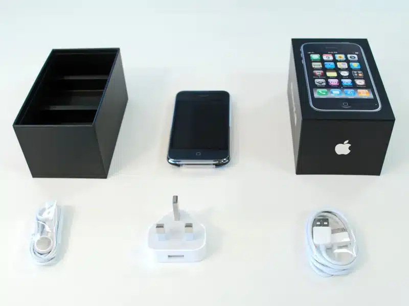
The unboxing – courtesy of iFixit
Apple “surprised” us early this month with the announcement of its iPhone 3G “s”. Whenever Apple releases a new device, everyone and their brother/sister has to get involved. Dr. Wreck is no exception and has been working hard with the team over at iFixit to get the details on the new device. Without further ado, here we go!
Teardown Process

Explosion – courtesy of iFixit
Those Apple Engineers really know how to pack a PCB. They’ve managed to fit almost everything onto the “top” of the main logic board. The 3Gs’ PCB makes the 3G’s PCB look sparse.

Applications Processor Core
Let’s take a minute to talk about the new Applications Processor Core. Apple has chosen to upgrade from the ARM 11 Samsung S3C6400 to the ARM A8 Samsung S5PC100 with this device.

iPhone 3Gs Block Diagram – In Progress
This is the single largest difference between the 3G and the 3Gs. Firstly, the manufacturing process has been reduced from 90nm to 65nm. Pipeline depth has been boosted to 13 stages from 8. More importantly, the clock speed of this newer processor is 600MHz, opposed to the 412MHz core of the old 3G. Samsung has also doubled the quantity of L1 cache from 16 to 32KB.
None of this even takes the new PowerVR graphics core into consideration. Apple is clearly thinking along the lines of a gaming device for this model. The SGX is fully programmable – like the graphics card on your PC or Mac. Expect some sweet gaming action in the near future.
@ 200MHz the SGX can pop 7M triangles/second and render 250M pixels/sec. That’s roughly 7 times the performance of the old MBX. It’s like comparing your old 486 to a Pentium.
Other Components

Moving around the rest of the PCB, it’s easy to notice the similarities with the previous 3G device. The Power Amp wins once again went to Triquint and Skyworks. We also see the NAND flash going to Toshiba, which as far as PhoneWreck is concerned is fairly surprising. The battery has been upgraded from the previous 1150mAh to 1219mAh, a much-needed upgrade. Only time will tell if Apple’s claim of increased battery life will hold.
The pseudo SRAM win goes to Numonyx. The BaseBand Processor appears to have similar markings to the previous 3G, so we can assume it’s an Infineon. This has been paired with the Infineon PMIC. The Applications Processor mentioned earlier (Samsung S5PC100) is paired with a PMIC courtesy of what appears to be NXP. It’s mounted with a DDR SDRAM coming in at 256MB.
True to form, Apple has re-branded some of the higher profile ICs we’re very interested in. We’ll be performing some more thorough analysis to further identify these.
Surprises Underneath

Underneath the logic board, we have a little surprise! A new combo chip from Broadcom (BCM4325). This chip packs 802.11a/b/g and Bluetooth 2.1 (+EDR and FM). This is a substantial change from the Marvel and CSR combo on the old 3G.
We’ve received some rumors and speculation about the other devices we weren’t able to ID. There is a guess from a few readers that the GPS chip may be the same as on the previous 3G – the Infineon Hammerhead II. This may be true, but the new package is a different size – this means that it could incorporate the compass hardware as well.
We’ve also heard rumors that the compass chip is the Asahi Kasei – AK8973. We’ll have to do some more digging to confirm this!
Conclusion

We’re currently in the process of performing a much more thorough analysis. Keep checking back for more details as they come – we’ll most likely be putting this device through its paces to see how it stacks up with the Palm Pre and BlackBerry Bold & Storm.
Thanks again to the wonderful people at iFixit for providing these great photos! If you want to see how it’s taken apart, make sure to check out their teardown.
Stay tuned and keep wrecking!